Following on from a previous post about this instrument, I discover a second fault.
Symptoms
It became apparent quite quickly when looking at S21 and S12 of a piece of wire with a ferrite bead on it, a symmetrical structure. The resulting traces should be identical, but they are not.
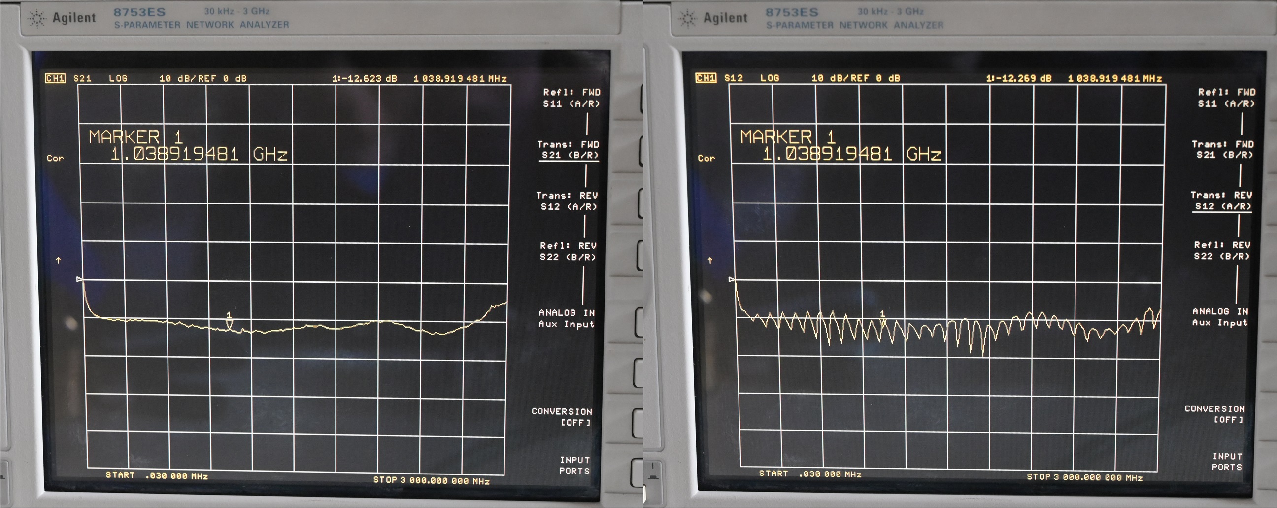
Unlike in my previous post were a significant effort was mounted to track down the problem, this time it’s not going to be so difficult. First thing to check was the output level of port 2 while the instrument is measuring S22. Could this crazy looking zig-zag response be a result of uneven output?
Diagnosis
I plugged port 2 into my spectrum analyser, slowed the sweep on the 8753ES down to about two seconds (so I can watch it from end to end) only to find that it’s a perfectly flat 0 dBm across the entire sweep. The issue must be with port 1.
I then set the instrument to measure S11, with the spectrum analyser attached to port 1 with the same two second sweep, once again measuring the output on my spectrum analyser, and I find that it’s attenuated by 20-30 dB. This is bad.
Looking at the block diagram of the instrument in the service manual, we can see that a likely culprit is the A24 transfer switch, whose exact part number is 5087-7067.
This part is clearly marked “STATIC SENSITIVE” thus I would not be surprised to find that it is at fault. I pulled it out of the instrument, hooked it up to a test supply & spectrum analyser and observed the same attenuation across it as was observed on port 1’s output. Fault located.

I had a quick look on eBay to see what the availability of this part is, and it’s bad news. It’s not quite as expensive as the A9 CPU board I was previously facing the prospect of having to buy, but it’s still very pricey. Worrying me further is that there are many dead units for sale, with port 1 marked as “BAD”, just the same as mine. One seller is describing them as “For repair”?

Realistically, could an ordinary person like myself repair one of these? Let’s open it up and have a look:

The components we’re looking at here are all control and power supply, none of which’ll be at fault. The faulty bit is inside the gold block – a proprietary hybrid. These usually aren’t even repairable by highly experienced, well equipped technicians as the dies within are not obtainable.
Rather than roll the dice on a very expensive second hand part off eBay, I’d rather see if I can make a replacement for this part. I’ll be detailing that effort in a separate post.
Repair
I started to put together a design based on what I could possibly assume about the existing switch, but feeling a bit unsure I decided to put the question to the EEVBlog forums and in an almost improbable turn of events, my question attracts a response from industry grandee Joel Dunsmore, the designer of the A24 transfer switch and quite a few other parts in this instrument. In a handful of posts – specifications, layout, design challenges are all revealed. He also made a suggestion about how I could return mine to life.
So I’m going to do just that.

At the input there is a diode string to prevent the switch some protection against ESD and power overloads. If these diodes are blown, they’ll attenuate the input as I’m seeing on mine. The theory is that if I simply pull this component out, the switch will be usable again, albeit with no input protection.

This technique successfully fixed the problem. I can no longer measure any loss through the switch, or to the termination when blocking. The big caveat of this solution is that port 1 is now extremely ESD sensitive. Beats being completely unusable.
Another problem???

Looking at the S11 “Open” measurement, something is still not right. The trace should be flat, but we’ve got some strange looking hump shape.
You guessed it. There’s another dead part in this instrument. Read the next repair story here.
Posted in Repair / modification, Test equipment
I had the same issue and did the same repair. I’m curious if there is any way to put in a new diode to add back some nominal ESD protection. Murata makes some low-capacitance diodes, but I’m guessing that they might clamp at too high of a voltage to give the needed protection. Any idea as to what the specifications of the original diodes might have been?
Nothing much was said about the diode other than it being a custom part. I’d guess its construction is what makes it exotic, not its properties as such. A single diode will clamp at +26dBm. So you need a few. How you gonna fit a chain in such a tiny space? 😛
I think that is why they made their own. I’ve got a dead switch here with two good diodes in it, but sheesh how to get them out intact and into the working switch. If you can figure that out – one’s all yours.
Thanks for the diode offer. I will need to come up with a way to do wire bonding before that will do me any good. I’m not there yet.
Currently working on a different machine, and what do you know – the same diode issue in the same location. Unfortunately, the test port coupler got really fried in this one. In addition burning out the 265 ohm resistor, it also burned out the line coming into the machine and melted it creating a short inside the connector. Of course, the switch diode was fried, but it also has a bad sampler board and a bad source. Clearly the seller took 4 broken units and made them into one lemon. Fixing the source may be difficult and it costs 3.5K – arguably more than the value of the machine. Frustrating.
It isn’t wire bonded I don’t think. Looked epoxy’d to me.
I reckon the sampler board should be easy to repair.
But a bad source. Ouch. The thought of that sends a chill down my spine. That’s a $1000 part right there. By the way if you attempt to repair it I would like to hear about it. I have seen dead 6GHz sources for sale cheaply on eBay from to time – would make a nice upgrade for mine if they’re actually repairable.
I ended up getting another “dead”ish unit and combining the source modules to create one working one. The amplifier was gone in one (inside of the main shielded box). In the other one, the variable attenuator was mucked up. There are something like 6 plug-and-play modules inside the source, so swapping this out was pretty easy). I sold the remaining dead source module (with the now known faults detailed & listed) on ebay for $600, so managed to come out allright in the end. The whole unit ended up being a parts unit, but I got it for just north of $1200 I think, so in the end when I had sold the parts the fix was more or less free.