
It’s no secret that EPROMs have great nostalgic value to me, and even today I include them in my projects where ever I can.
For many years now I’ve had a set of the worlds’ first ever commercially available EPROM – the 1702A, sitting in a piece of anti-static foam, waiting to be used once again.
As I’ve long been aware this would be a tall order, because this is a particularly difficult EPROM to program. There are no commercially available programmers and second hand programmers are practically unobtainable. Even if you could obtain one, you may find that is quite large, heavy and difficult to use, perhaps having to program each byte by hand.

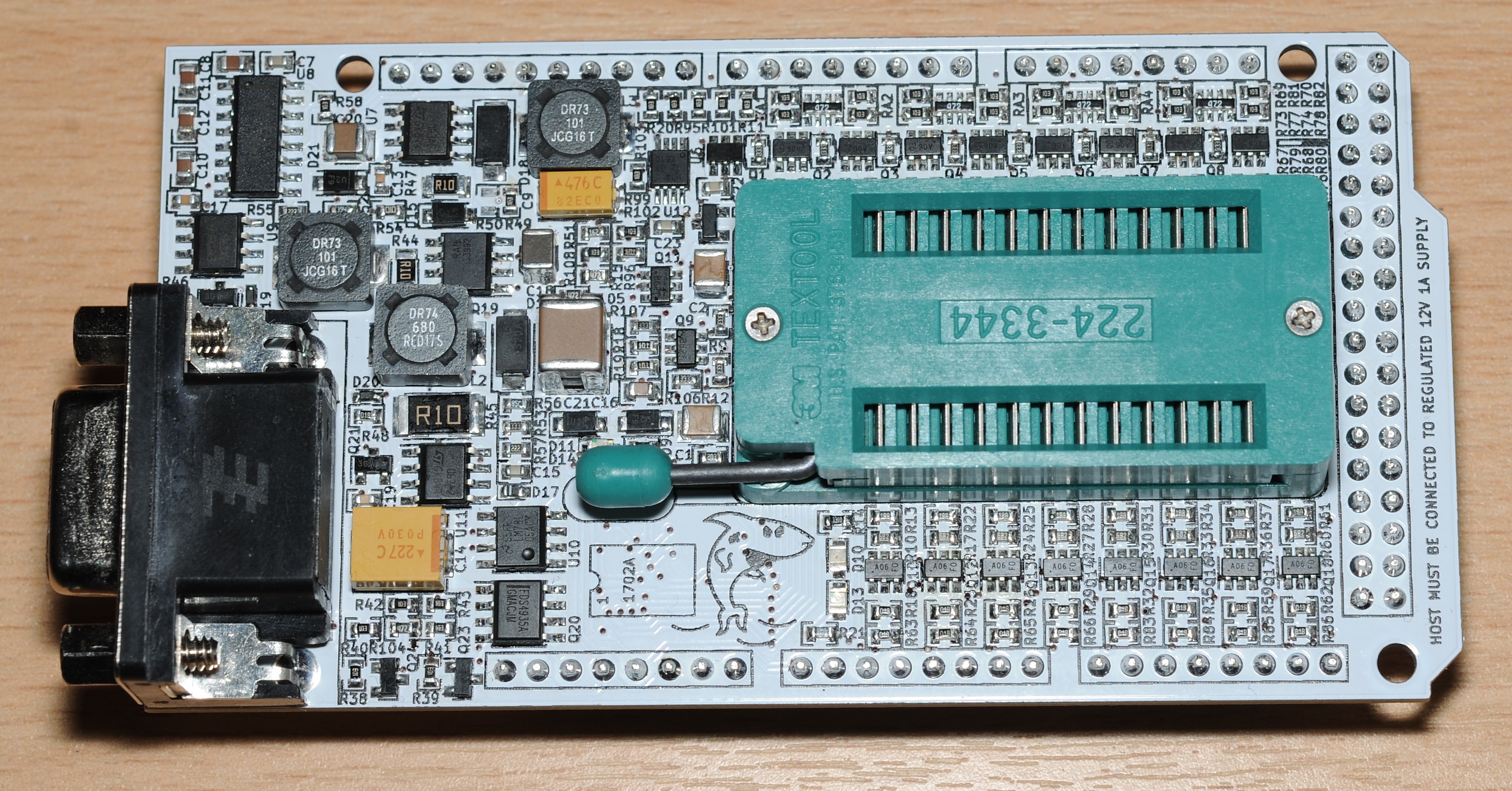
This has turned out to be a very tempting idea for a project – a small, compact, easy to use 1702A programmer which interfaces with modern computers.
Fortunately availability of 1702A type devices is actually quite good. I was able to obtain a number of them from eBay for fairly reasonable sums.

Design Details
I’m not going to go into the detail of programming these devices. This has been done at length on this page. Instead let’s focus on how my design differs from other two-socket designs of which there are a few already on the internet.
Single power supply
Because reading and writing the 1702A requires a cornucopia of different voltages, D.I.Y. programmers are often found to have perhaps three or four different power supplies hanging off them. This is of course a little inconvenient and certainly something I wanted to avoid. My design achieves this with three on-board switching (step-up + inverting) regulators.
Single socket operation
The reason for using two sockets is that the voltages used for reading and writing are so completely different that it becomes difficult to do both on the same socket.
Clearly it is possible because the original design from Intel did do this, as did others of the day. Mine does not share much in common with that design, except for the drivers for the data pins, a less than perfect, but tricky bit of circuitry which I was not able to improve upon.
SMD or through-hole?
I did consider building this as a through-hole design however with 204 components this was going to end up quite large and difficult to lay out. In fact it would likely end up with more than 220 components in a through-hole design due to some of the dual transistor parts I’ve used not being available in through-hole packages.
Here is an example of a dual socket programmer in through-hole. My single socket design would have been considerably larger.
Physical form factor
I decided to build it as an Arduino mega shield, mainly so I could use it on my previously constructed 8086 Arduino contraption (The reason it has a DE-9 RS-232 connector fitted, this board does not have USB to serial like the Arduino)
Another reason for this form is because if attached to an Arduino, this reduces the overall size even further.
Building one yourself
If you have a sound understanding of how these devices are programmed, are well equipped and have very good soldering and troubleshooting skills – everything you need to build one is provided below.
Update: I was rather surprised to find that people are actually building these things. There are now three others that I am aware of:


If you go to the trouble of building one, let me know about it. I enjoy seeing them 😉
Host software / firmware
Please see the main project page for more information.
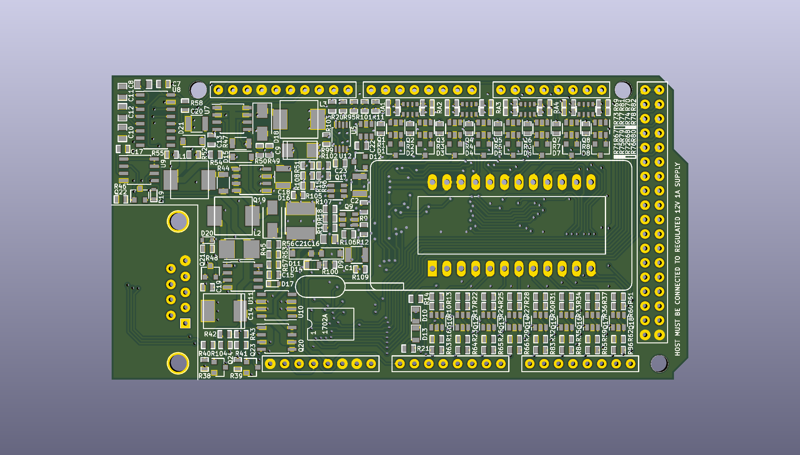
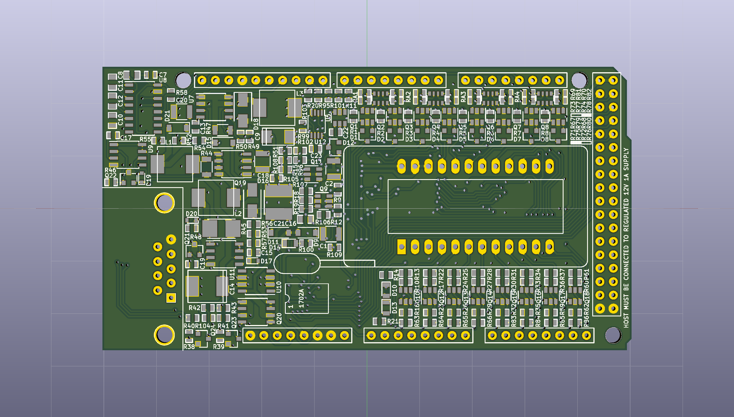
Schematic
- Can be downloaded from here.
- You can also see the schematic for the reader board seen in the YouTube video here.
Gerbers
There are two version of gerbers for this board.
- “Long” version – which has the exact dimensions of the Arduino mega PCB. It’s 101.5mm x 53.5mm in size, which is over the 100×100 limit of seeedstudio’s $4 PCB service. Use this gerber if using a PCB house that doesn’t charge a lot more for exceeding 100mm (image).
- “Short” version – which has the tab at the end of the board cropped a little. It’s 99.95mm x 53.5mm in size (image).
Neither version includes any signatures or graphics seen in my photos. Those are for my boards only 😉
BOM
A complete BOM can be downloaded here. Exact part numbers for special components are specified, however generic stuff such as resistors and capacitors are not. Up to you to choose those.
Hello
This is Hassan from Pakistan. I am an electronics engineer and came across a vintahe eprom Part#: AM1702 OR MM1702. I see that you have its programmer. Can you please share price and details of this programmer
BR
Hassan
Hi. They are not for sale.
Hassan,
Please note that the programming algorithm for 1702 EPROMs is different than the algorithm for 1702A EPROMs, so this programmer probably will not work with your AM1702 and MM1702 EPROMs.
Once again – it worked on the first try! Matt, you are a genius!
Thanks and I did not forget to mention you on my website: http://www.wolfgangrobel.de/programmer/ardprog.htm
Cheers for the link! I always enjoy seeing photos of my programmer built by others!
Hey, Wolfgang! I sold that the old Prolog M900 (#2 with case) to somebody in Germany on ebay several years ago.
I like this idea, but that is a lot of tiny SMC components to mount. Have you considered splitting the circuit into two boards that can stack on top of each other? That is, a lower and upper board that stack on top of the Arduino Mega, that way you can use through hole components (especially those transistors and caps). If you keep each one under a 100×100 mm^2 the cost is a lot cheaper than making a larger board.
You would probably need to stack it 5 or 6 high to get everything on there. 4 layer PCBs would probably also be required because the routing between components and interconnects would be so complicated. It would be a very expensive and zany contraption indeed.
I have pondered a through-hole version of it. I worked out that it would be quite large, so large that basing it on an Arduino wouldn’t make sense.
Fair enough. Mind if I take a crack at it?
Do it. Drop me an email. I have a list of things to consider. Email on the about page
Hi Charles,
I must apologise Matt for being “off topic” here, I have a query relating to the PCB board shown on your web pages that is a Mega2560 shield EPROM Programmer and a link to your eBay site to purchase a blank board. That link does not go to your board, nor can I find it any where else.
Are you still selling these multi-eprom boards? If yes, how can I purchase one?
Apologies for hijacking your conversation.
I used an Intel EPROM programmer in 1973 to program a 1702A in Melbourne, Australia. I used it to generate a monitor program for my SCMP prototyping board (256bytes exactly). Dead bug wired it into the system. 16 Hex+Fn keys, and 6 character bubble 7 Seg display. Intel had an outlet in Swanston St Carlton, just up from Melbourne Uni where I was studying. I had to hand enter and program the code in their waiting room, as I was not allowed to borrow their programmer. I am impressed with your endeavours here. I still have my only 1702A and SCMP CPU, both ceramic+gold pins!. I am wanting to program 2764A EPROMs for a SYM-1.
Hi! This looks like a fun project to put together and useful to diagnose an old computer I have come across. I am looking forward to putting it together. Would you mind clarifying the values for caps, C3, etc, and C8, etc? The BOM and schematic simply say 0.1 and 1.
Can’t be too careful when working with old eproms such as these.
Thank you. 🙂
Both in uF
Hi again! =)
Back in July 2022 I wasn’t able to source all the parts due to what was going on in the world around then. For reasons, I have decided to pick this back up!
I am having trouble with one part, D17. I am finding it difficult to find a diode in stock with a forward drop curve entirely above 0.6v. Will a CDSER4448 work in a pinch? It is the closet I can find on Mouser.
Higher voltage drop is preferable, but I don’t think you’ll have any troubles. It will work even if you bypass the diode entirely, it’s just not ideal.
Hi! 😀 I am the guy wit the two socket programmer… you linked to my youtube video 😀 Thanks for that!! That version actually blew up with a big “booom” and almost killed my laptop. That’s why I am now (after 5 years) giving up because of lack of time and trying to build yours!
Some of the MOSFETs however, I could not buy anymore…. I tried to find a replacement. Could you tell me if:
Instead of the FDS3992 (rated for IDS = 4.5A), a ZXMN10A08DN8TACT-ND (same specs except IDS = 1.2A) will work for Q19? I could not find any with 4.5A 🙁
This will be my first real SMD solder project… I hope I won’t generate a big blobb… XD
So long as it has the same footprint and pinout. I used FDS3992 because I already had a strip of them. It’s overkill spec for the application.
By the way was yours based on the Tronola design?
Yes, I wanted to cooperate with him on this, introducing an Atmega as a micro controller and switching the read and write power supplies on the fly with relays, however, after my project almost burnt, my father died two years later and I was very busy, so I had no chance on improving it.
Sorry to hear that. Well hopefully it’ll go better this time.
I do rather like how few components Steve Lafferty’s design has. What you were trying to do there i.e. swap the PP control for a microcontroller on his design is an idea I really think has legs. By comparison mine has an absolutely ridiculous number of (tiny) components. It was originally built as a bit of a joke. I didn’t think anyone else would attempt it so wasn’t worried about ease of construction for others.
I may try and simplify it in future. Maybe even re-do it as a through-hole design too but I would prefer to stick to single socket thus it will still be quite large and complicated.
From a quick look on Mouser FDS3992 is still in production but out of stock? Was that your finding?
Yes, I didn’t want to wait for months or even till end of next year… rather in the order of weeks 🙂 If you intended it as a joke, it is a very good and obviously working joke. I found, there is no marking on how to orientate all the diodes. I will have to look with the help of the schematics on how to install them 😛 I tried to also generate my voltages out of a single voltage, but all simulations in LTSpice failed. MOSFET circuit design is not one of my favorites, nor could I design a working buck-boost converter with a 555. Your voltage circuits also invert some of my ideas and simplify them. In the end I just want to burn some of my 1702A for a Busicom Calculator Replica I am developing (with 4289 and some LCD instead of the drum printer).
Also there seems to be a wrong symbol in your schematics. Q19A and Q19B are both N-Channel if the 3992 is used. However, in the schematics, one symbol is a P-Channel. That does not make sense to me. I trust the part list and the picture of the completed device! I am already building one.
FInished building, does not work… instead of -9V, I get 0.57V…. This will be painful to debug 🙁
I found the problem… you told me about the pinout of the alternate parts *stupid*, and I checked every part except one and of course that one ha a wrong pinout (Q11 and Q9). Now since I cannot get ones with fitting layout I will try to fix it with thin copper wires… this is hardcore 🙂
IT WORKS IT WORKS IT WORKS oO I just wrote my first 1702A… THANK YOU THANK YOU THANK YOU !!!!!
Drop me a picture of it. I’d love to put it in the gallery.
Hi,
Are the below k-ohm?
R13 R22 R25 R28 R31 R34 R37 R61 8 150
R14 R21 R100 3 330
R18 R19 R102 3 100
Ohm
Assume when stated resistors are SM0603:SM0603, this is case style inch?
SM0603 mm case style looks too small for the solder pads?
Hi,
My eyes are not good enough so that I can assemble myself and so I am getting the devie assembled by a company and I need to provide component polarity and pin1 placement, I dont see a dot or marker, whats your key to placement?
Cheers
Chris
Just ordered a stack (5pcs) of each of the “programmer” series (MCS48, HVPROM, 27xx and 1702A) from JLCPCB.. 5/ea with shipping to the U.S. for $48, not bad. And those are the “long” versions; they did not charge extra.
Will build and test all, and then will upload pics to the proper pages.
Fred
I’m curious why the VBB supply appears so robust. The old 1977 Intel Memory Design Handbook lists IBB as 10 mA typical. There’s also the note “The VBB supply must be limited to 100 mA max current to prevent damage to the device”. FWIW I took a look at the Feb. ’78 Popular Electronics design and it appears the Zener regulated VBB cuts out at about 19.5 mA. Did I miss something in the schematic?
Today I programmed my first eprom 1702A with Matt’s project.
Beautiful project, thanks Matt.