In my previous post I found that a mystery mixer IC was in fact the age-old TCA240 flying under a different part number. Today I’m going to take a closer look at this very early device.

Unlike modern chips whose datasheets can stretch to a hundred pages, typically handholding engineers from start to finish, the TCA240 datasheet is just 7 pages long, throwing us straight in the deep end without asking us if we can swim.
In an attempt to try understand it I’m interested to see I can build something with it. But first, let’s try and break it open with a calculator.
DC Analysis
As we saw previously, there is very little inside this chip. This however, does not mean it is going to be simple to understand. It is essentially a matched pair of cascode amplifiers but with multiple inputs. “TR4” (herein Q4) is intended only for setting the quiescent current. “D1” and “R1” are a rather interesting feature, making it difficult to work out how to calculate it. Frustratingly the datasheet says nothing about D1.
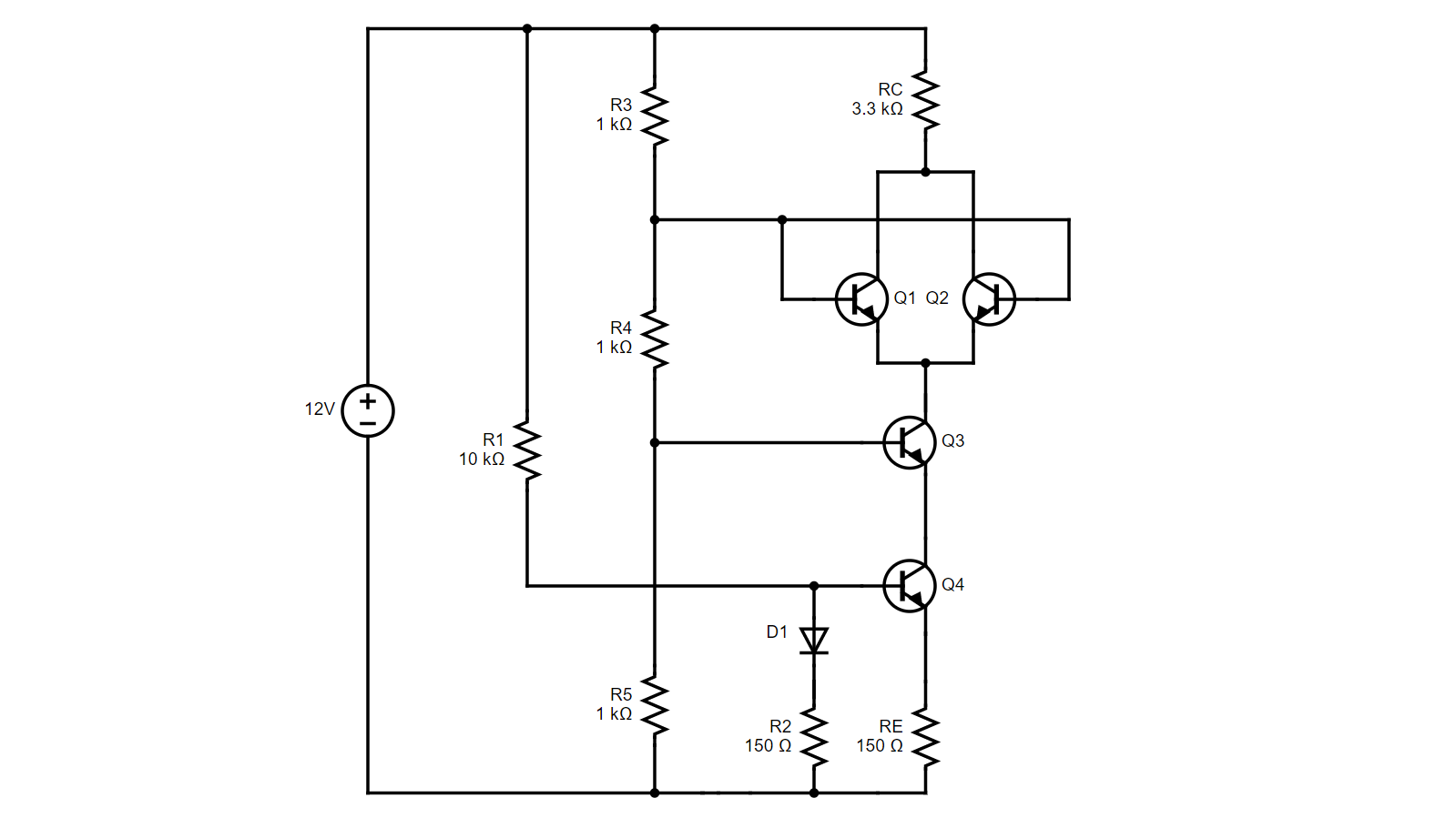
So what do we do about this mystery nonlinear component in the circuit? If we are to assume that R2/D1 and RE/Q4 are symmetrical structures, with D1 being the same type of P-N junction used for Q4, things get a bit easier:
![\[V_B_(_Q_4_) \approx V_S \frac{R_2}{R_2+R_1} + V_B_E\]](https://www.mattmillman.com/wp-content/ql-cache/quicklatex.com-e4e8a6f0ec3e082d092de9809cb3649c_l3.png "Rendered by QuickLaTeX.com")
The above cannot be absolutely true as the junctions inevitably will differ. Practical experimentation gives a result within 3% of the above. Good enough to move on.
Normally when calculating IE we would subtract VBE from VB but since it was just added, VBE can be eliminated from the equation. Leaving us with:
![\[I_S \approx I_E_(_Q_4_) \approx \frac{V_S \frac{R_2}{R_2+R_1}}{R_E}\]](https://www.mattmillman.com/wp-content/ql-cache/quicklatex.com-9aa1607b15147a429fb81705a86dbaae_l3.png "Rendered by QuickLaTeX.com")
The above also bundles in the neglable IB(Q4) finally giving IS. This figure is the constant current through this half of the IC. The calculated value is 1.18 mA in this example.
The TCA240 is typically biased using a three-resistor network (R3, R4 and R5) in the above diagram. In the below calculation VC is the connection between RC and the collectors of Q1/Q2:
![\[V_C_(_Q_1_) = \frac{V_S \times \left ( R_3 + R_4 \right )}{R_3+R_4+R_5} + V_B_E\]](https://www.mattmillman.com/wp-content/ql-cache/quicklatex.com-16bd4985f02229f7e4404b8473c9c1ec_l3.png "Rendered by QuickLaTeX.com")
VBE is assumed to be 0.7V and equal for all transistors. The above gives an estimate of 8.7 volts, which is exactly what I observed on the physical circuit.
VC (Q3) cannot be measured, but for reference:
![\[V_C_(_Q_3_) = \frac{V_S \times R_3}{R_3+R_4+R_5} + V_B_E\]](https://www.mattmillman.com/wp-content/ql-cache/quicklatex.com-b67d4eda5b773d41fd0953de22561eec_l3.png "Rendered by QuickLaTeX.com")
(4.7 V)
Finally, for reference – Q4 being a current source its VC can be calculated as:
![\[V_C_(_Q_4_) = V_S - V_C_E_(_M_) -V_C_E_(_Q_4_)\]](https://www.mattmillman.com/wp-content/ql-cache/quicklatex.com-dac31958737f4985a2d0fb90e3645b3f_l3.png "Rendered by QuickLaTeX.com")
![\[V_C_E_(_Q_4_) \approx V_S - V_C_E_(_M_) - I_S \left ( R_C + R_E \right )\]](https://www.mattmillman.com/wp-content/ql-cache/quicklatex.com-160ca67ae79e7da482780c7ff1cb22fb_l3.png "Rendered by QuickLaTeX.com")
![\[V_C_E_(_M_) = \min \{ V_C_E_(_Q_1_), V_C_E_(_Q_2_) \} + V_C_E_(_Q_3_)\]](https://www.mattmillman.com/wp-content/ql-cache/quicklatex.com-8be835e92b16c5c6e6a54489b56d7edc_l3.png "Rendered by QuickLaTeX.com")
i.e. whatever voltage is required to maintain a constant current (IS) through the circuit. Not something to dwell on. I just used this to verify the rest of my workings.
DC Analysis conclusion
The above reveals that operation similar to that of a common emitter amplifier, however instead of a half-way voltage split, the biasing arrangement splits VS into thirds to provide sufficient headroom for the two tiers of the circuit (Q1/2 and Q3). Q4 provides a constant current source to compensate for the differing input signals.
AC Analysis
Originally I had planned to delve into the AC theory of this chip, but, err… this has already taken way too much of my time. So instead I’m going to jump right in and build something. Now that I know how to bias it properly I should be able to get something out of it.
Building something with it

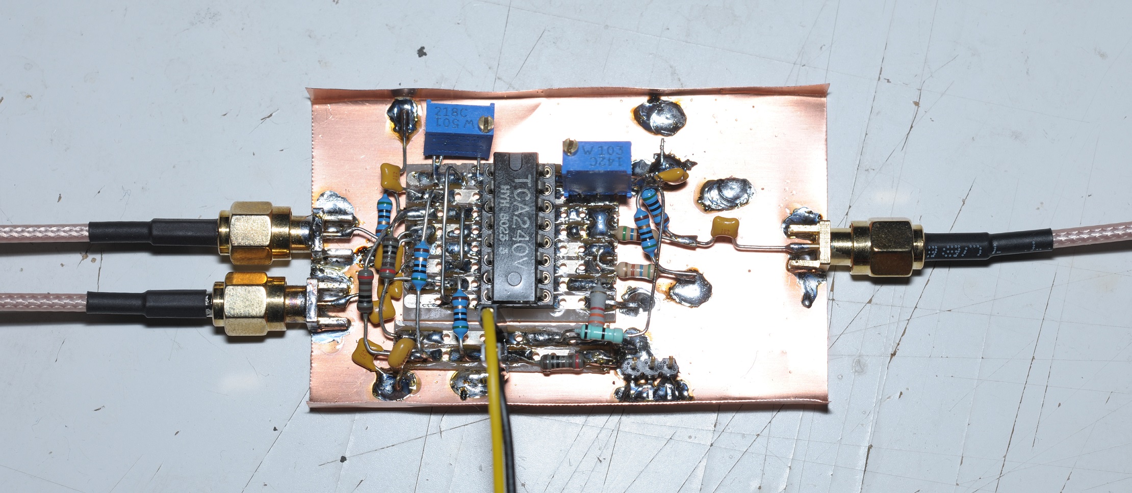
For my test I’ll be using the above circuit. I found it floating around on the internet. It’s probably from an old databook however I was unable to find the original source. Additionally – I’ve mucked it around quite a bit in MS paint. The original is on my previous post.
Inputs are now both approximately 50Ω. Output is sort-of 50Ω too. This chip is ultimately designed to work with impedances in the several kΩ range so the above is quite a fudge. The current setting resistors have been decreased to 3.3K which according to the previous calculation gives a constant current of 3.47 mA.
I tried pushing it harder. It doesn’t work, so this seems to be the max. The output is picked off a matching network giving a weak 50Ω source. This wastes most of the mixers potential power but is good enough to attach to a spectrum analyser. Ideally one would use a Balun or post-amplification to better match to this part however I don’t have anything suitable to hand.
The 50/560Ω resistor divider on the collectors is taken from the TCA240 datasheet. I worked out that these values are chosen because they yield around 8.7V on the collectors of the current source transistors when the mixer transistors are saturated.

The output on the spectrum analyser was pretty much as expected. There are three dominant tones on the output, the left is the “minus” product at 20 MHz, the carrier tone in the centre at 25 MHz and the “plus” product is at 30 MHz on the right.
The circuit is intended to suppress the carrier tone, and it does however it appears at quite a high amplitude on my test because I’ve pissed away so much of the potential power with a poor output matching arrangement, leaving radiated / parasitic coupling of the carrier tone quite high in relative amplitude.
So what have I learned here?

The purpose of this exercise it to work out what all of the adjustments are on my vintage DQPSK modulator. I now have another two (from the I/Q mixers block):
- “Balance” (R7) should be adjusted until the carrier tone is as at the lowest amplitude possible. If the constant current of the two halves of the mixer are unbalanced, the amplitude of the carrier tone increases.
- The adjustment across pins 1-8 turns out to be to control the gain of the mixer. This ultimately is to allow the amplitude of I and Q to be equalised.
More to come…
Posted in Circuit snippets