During the early phases of this project, I spent quite a bit of time reading around the internets about prospective homebrew 8086 projects and it seems I am not the first person to have thought of something like this. The appeal is clear: building a microcomputer based on such a historically significant processor is a very interesting project indeed.


But to achieve it? Well that is quite something else. To give an indication – take a look at this monster, I too constantly found myself reaching for the lesser 8088, with its 8 bit front side bus, this dramatically decreases this physical complexity, or even an 8086 based microcontroller like the esoteric 80186, or completely copping out and walking the path of least resistance: The 80188. At that point I might as well have just built something based on an 8051.
With the easy options relatively historically obscure, and this being purely a project of interest, it had to be an 8086, and to produce it in something that could pass its self off as an Arduino left me with several mountains to climb.

1: CPU
The board is designed to support all variants of the 8086: 8086, 8086-2 and 8086-1, clocked at 5, 8 and 10MHz respectively. 80C86 parts work OK too. A jumper is included to select the clock frequency.
2: ROM
The 8086 being a pure 16-bit processor, requires that its boot ROM is a 16-bit device, so either I’ve got to have two 8-bit chips side by side (more common), or a single 16-bit. I’ve decided to keep it retro and use a 16-bit 27C4002 EPROM, a variant of the popular 8-bit 27C4001.
Fortunately for this project, there is still an awful lot of EPROMs in the world.
The EPROM is only used for the bootloader which performs booting/programming of the SPI serial flash chip. There’s nothing to prevent the system from being run entirely from EPROM (my original plan) but in practise, it’s a bit of a pain; as it requires an EPROM eraser, programmer, tube of 27C4002’s, and quite a bit of patience.
3: CPLD
The CPLD is the heart of this gizmo, and is the reason it isn’t table mat sized with dozens of logic chips.
Providing (of the features I originally planned):
- Address/data demux
- 54 General purpose pins
- 38 of which are Input/Output
- 4 of which include port change interrupt functionality
- 2 can be configured as external interrupts
- The remaining 16 are output only
- UART/GPIO multiplexing for the four UARTs
- I/O address decoding: four UARTs, SPI Master and the CPLD’s internal registers
- Memory address decoding: EPROM and SRAM
- Basic programmable interrupt controller
- A single 16-bit timer with fixed 1:128 prescaler
- The mandatory i8284
Some planned features had to be omitted due to limitations of CPLD capacity:
- PWM outputs
- A better interrupt controller, closer to the i8259
- all 70 (General purpose + ADC) pins as full Input/Output
- Ability to configure timer prescaler
When I selected XC95216 for this design 6 months ago, it was the most suitable for what I was trying to accomplish, and fitted in with the constraints presented. I was also aware that it was end of life, but back then, this project was just a silly thing that was just going to be for me, so I didn’t really mind. Going forward, this could be somewhat of a problem; which thus far, I’ve not decided how I’m going to tackle. Every option I’ve looked at so far either compromises the elegance of the design, or dramatically ratchets up the cost.

By rough estimates, with 65% of Pterms in use – 3,120 of the 4,800 available logic gates are utilised in 8OD’s PLD. Unfortunately, with 91% of interconnects and 99% of Macrocells in use: This thing is full.
4: SRAM
A very generous amount of SRAM is included, which is the only writeable RAM the CPU has available to it. The chip I’ve selected is 16 bits wide and 512KB in size, occupying half of the 8086’s 1MB address space.
5: UARTs
Because serial communication is pretty important to Microcontrollers, I’ve been generous. This tiny little chip is a 16C554, which is four 16C550’s stuffed in one package. Their interrupts are routed to the CPU, and RX/TX lines to the General purpose headers, all via the CPLD. Additionally, the flow control signals are made available on a dedicated 10-pin header.
6: SPI
The largest change to 8OD.1 was the addition of a dedicated SPI master – TP3465, one of those chips I never thought would exist, and indeed spent a wedge of time learning the existence of.
8OD.0 did SPI with an assisted bit-at-a-time master implemented in the CPLD who’s performance was poor. Even with an FPGA, implementing a competent, good performing SPI master would be a challenge, as SPI has quite a few modes and quirks that have to be supported. TP3465, branding its self as a Microwire master, is a very competent SPI master which thus far has left nothing to be desired. I’d have been in a bit of hot water had it not existed.
7: Analog to Digital
An AD7490 from Analog Devices is included which provides the sixteen ADC channels, with the exception that this design is 12-bit instead of the AVR’s 10-bit. One limitation here is that AVRs can re-purpose their ADC pins as GPIO, whereas this board cannot. 8OD.0 was designed to accommodate this but it had to be removed in 8OD.1 to reduce PCB clutter and free up capacity in the CPLD.
8: SPI Flash memory
1 Megabyte of flash memory is included. More about that here.
I2C
The first and second revisions of 8OD had no I2C, because I couldn’t implement anything remotely satisfactory in the CPLD (other than bit-bang) and I didn’t think it’d be possible to cram a dedicated chip on the board either.
After many weeks of toil re-arranging the board I managed to squeeze a PCF8584 hardware I2C master on the third revision of the board, giving it an elegant and good performing I2C solution.
Shield Compatibility
Despite my best efforts, there’s limitations. Most shields should work, but some wont be compatible.
The limitations are:
- There aren’t any PWM outputs
- External interrupts are only on pins 2 and 3
- Port change interrupt is only for pins 8 through 11
- ADC pins are ADC only. The cannot be re-purposed as GPIO
- Pins 38 through 53 are output only
PCB
It’s double sided (2 layer).

Form Factor
8OD is designed to with an identical header layout to the Arduino Mega 2560 R3.
The Mega 2560 is able to expose a local bus on the 36-pin header – a planned feature for 8OD (with different CPLD build).

Shields which occupy the Arduino Mega 2560 R3’s full header set are very rare.
Schematic
Also, check out the top level CPLD schematic.
Is it fully working?
The largest area of effort has been answering this question. Realising that it was unlikely that I’d get something like this right first time, a single prototype (8OD.0), was built around mid 2014 followed by 4 months verification using the following:
- ISim VHDL Test benches (completed before prototype construction)
- Many weeks testing and tweaking the physical board with logic analyser attached
- Checking all on-board signals by oscilloscope during operation
- Final stage of design verification running a few test applications

Predictably: 8OD.0 had many defects, thanks mostly to not properly understanding the 8086, as well as trying to jam too much stuff in the PLD.

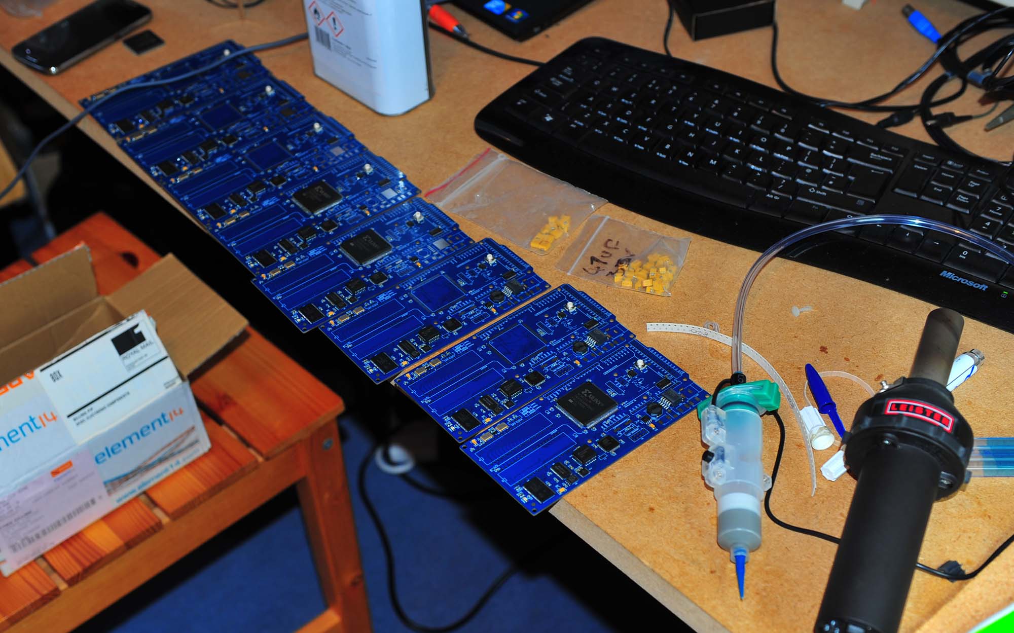
The current board is 8OD.1 (blue) which fixes all of the mistakes I’ve found in 8OD.0. It is very similar (if not identical) to what will go into production (assuming it ever does…).
Oh, man. I’ve been wanting to do something exactly like this for years. I was even gathering the parts.
Kudos to you!
— Zach
This project is really awesome! For a long time I’ve been planning to do something similar but with a TMS9900 that my Dad bought for a DIY home computer project in the 70s (but never actually got around to building). Your project provides some great inspiration to how to mix an old processor with new support chips, something I’ve idly wondered about from time to time. Thanks for taking the time to write up the project so well!
Yeah it would be cool to do something like that, but the problem for me is that TMS9900 is a lot more obscure, and wouldn’t be found interesting by very many people other than me 😉
Ok, I’ve read through this and the related pages and i’m still not quite sure i get it. Does the 8086 have direct access to the rom/ram or is everything mediated through the cpld?
The CPLD doesn’t mediate the bus at all. It does the following in terms of RAM/ROM access:
1) Chip select decoding (based on A19 for RAM/ROM)
2) Replaces the 2x 74LS373’s that are normally used to demux address/data bus.
3) It also latches A16 to A19, and the BHE signal, which annoyingly, tristate during the second half of a memory access. (this would normally be done with a third 74LS373)
Nothing else. The story is quite different for I/O though.
how does the 8086 execute from the flash?
It doesn’t execute from flash directly.
When powered on, it executes from the EPROM, which has code that copies the HEX file from the SPI flash into RAM, then it jumps to RAM and runs from there.
This process is pretty quick. Typical images complete the load under 50ms.
Matt: is there an application note or something that talks about using the microwire controller has an SPI interface?
Not quite sure what you are asking here? Are you wondering how I’m using a Microwire controller for SPI? If so, easy. They’re the same thing.
SPI Technically has a few more modes which include 8/16 data, clock polarity, skew etc. TP3465 supports all of this so technically it’s a full SPI controller. It is also very old chip possibly pre-dating the term ‘SPI’
(yes, I know I’m replying to a 4 month old thread…)
I’m pretty sure what you’re bumping into here is that National Semi (gobbled up by TI) and Motorola (later Freescale, then gobbled up by NXP) were competitors. NS marketed Microwire, and Moto marketed SPI. You’re right; SPI grew “modes” and such, while Microwire stayed pretty much the same.
I never knew about the TP3465 – wish I had when I made my HD6309 SBC a while back. Instead, I implemented a SPI master in my CPLD at the expense of a lot of macrocells.
Finally – nice work on the 8086 SBC. If ever a chip was made in anticipation of programmable logic to make it usable, the 8086/88 has to be it. Ghastly bus brings back nightmares… Your trials and tribulations with getting it running weren’t caused by the CPLD – it was a real PITA to get it running anyhow. Hats off!
I really like this board, how to buy it ?
Hello.
It is not for sale.
Hello,
Can You share gerber files for this board ?
Can You share source code for this beautiful project ?
Best Regarrds
Hello,
Can You share gerber files for this board ?
Can You share source code for this beautiful project ?
Can You share file for CPLD ?
Best Regarrds
The source code is available for download on the Software section
What exactly would you do with the Gerbers and CPLD source ?
Hello,
Can You share files for this 8080 board ?
Best Regards
How to burn code there? And is it available to purchase?
which code? I probably have a board or two I could sell off.