
Introduction
To compliment the recent publication of my MCS-48 programmer shield, I thought it’d be interesting to build something useful based on one of these. Completed in 1976, the MCS-48 is 44 years old at the time of writing this article, giving us an opportunity to venture back into the distant past of embedded development, peeling away the many layers of hardware and software we typically float atop of on the likes of Arduino and Raspberry Pi.

With the prospect of building ones own gizmo based on the very first microcontroller – the TMS1000 hovering just a hair above zero, the MCS-48 offers us a decent consolation.
Unlike the almost equally ancient MCS-51 which refuses to die, industry decided to leave MCS-48 in the past. When looking at the details, it looks likely that the efforts of the MCS-48 project went into the MCS-51, however the two have neither instruction set, or pin compatibility. As such, MCS-48 does not have any modern descendants or tooling. With such a limited instruction set and no data stack, writing 3GL compilers for it would have been challenging, and resulting code would have been very wasteful of its limited resources.
For a microcontroller with only GPIOs a single timer, 1K of program space and 64 bytes of data memory (32 depending on how you count it), it can be a bit of a stretch to think of something useful to do with it. This dual temperature sensor doesn’t need anything more, and it’s something I could just about bear the thought of programming in its assembler language, as there is not any other choice.
Software development
As I hinted to earlier, there is no C compiler for MCS-48, making writing software for these devices challenging. It is stated on Wikipedia that a PL/M compiler was available for these however I was unable find it or any other mention. To add to the pain, there’s no hardware multiply, divide or subtract either. There isn’t even an instruction for comparing two numbers. All of this has to be pieced together with primitive logic instructions. As I worked my way through the implementation, I kept telling myself it would get easier. It didn’t.
Even being equipped with a proper logic analyser, using modern PCs, editors and a very easy to use programmer, writing the software for this was still very difficult. It took me nearly three weeks to complete it, whereas an 8051 version (C/Keil implementation) of this same project I completed 7 years earlier was completed in under two days.

I cheated a little by using a modern enthusiast-built assembler – ASM48 for this project.
Back in 1977, when these were first purchasable, there were no PCs or DOS to write the software on. A purpose built machine, the Intel MDS-II (microprocessor development platform) with an assembler also from Intel was used. Some scanned manuals I’ve found show that the assembler outputs the following version string:
ISIS-II MCS-48/UPI-41 MACRO ASSEMBLER, V3.0
This may be a copy of it here. The MDS-II ran a special operating system called ISIS-II. It is suspected (although not confirmed) that IBM developed the original PC BIOS on one of these machines too (they certainly did not develop it on a PC), there is an interesting thread about that here, which details the challenges of recovering these early development tools.
You can see the MDS-II pictured in the image below (blue, on the left).
#/media/File:Intel_MDS.jpg)
There is also a simulator for the ISIS-II platform. A potential interesting re-visit for the future.
Programming an MCS-48
Internal EPROM MCS-48’s cannot be programmed in standard EPROM programmers. They require a specially designed programmer. Hardware is still obtainable for however not particularly cheap. I went to the trouble of building my own programmer, in the form of an Arduino shield.

In addition to the programmer, an EPROM eraser is also required. Mine is a classic design from the 1980s however there are plenty of cheapy Chinese units for sale on eBay these days.

Debugging
Typical debug techniques used on modern microcontrollers, for example printf() or in-circuit debugging are out of the question. An emulator would have been of little practical use as these devices almost always needed to be debugged in-situ.
Assuming you weren’t building a product that could be physically damaged by stopping the processor, the “austere” approach recommended by the databook is to use a romless version with a single step circuit, combined with the SS (single step) pin to step through your code with an external logic analyser attached to an external EPROMs address/data signals.
With this you can see what the program counter is up to, but you have no idea what any of the registers inside the CPU contain. If you need to see one of those, you have to copy it into the accumulator, then write it out onto the bus, assuming that doing so didn’t cause some kind of catastrophe, then capturing it with a logic analyser.

Well equipped engineers of the day may have been in possession of one of the above. The ICE-48 simulator was connected in place of a 40 pin MCS-48, allowing engineers to view the contents of internal registers, set breakpoints and single step. Quite a luxury compared with my experiences.
I found that the easiest way to debug an MCS-48 is to not debug it at all. Instead I repeatedly ran the instructions through in my head over and over again, and tried to get it right first time. This is a lot less time consuming that any other approach.
A little joke, at my expense
At the outset of this project I purchased an MCS-48 databook off eBay (I just wanted to have one). What I received was the original 1976 edition, which, has errors in it. Damned eBay rubbish strikes again.
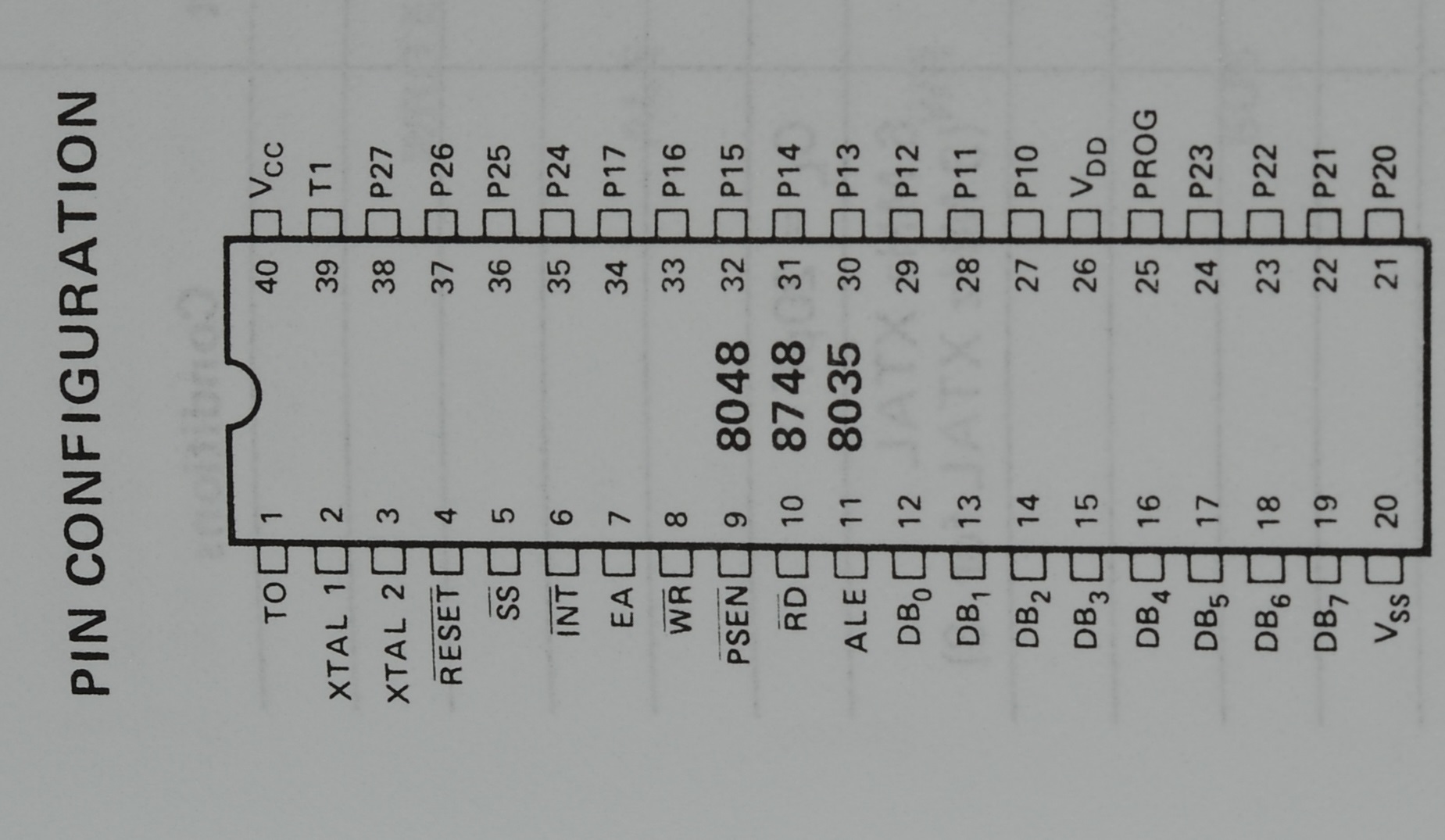
Above is the stated MCS-48 pinout, which is incorrect. The RD/WR pins are shown swapped. My first revision of the schematic included this mistake, because I worked from this book. This lead to a lot of head scratching when I first attempted to debug it on my logic analyser.
Taming the Quasi-Bidirectional GPIO
On modern microcontrollers GPIOs are easy. We have register which can enable a pair of P/Nch FETs for use as an output, typically being able to sink and source a fairly decent amount of current, usually enough to power LEDs and small relays for example.
On the MCS-48, we are lumbered with the quasi-bidirectional GPIO. The databook makes a lot of how wonderful and innovative these are but from the perspective of having used modern ‘true’ GPIOs – they are a pain in the backside.

Essentially these are both an input and an output at the same time. The input part is simply a buffer which is always sampling the external pin, and the output part is an N-ch FET which pulls the pin low, with an internal 50K pull-up providing the logic “high”. There is also a puny P-ch FET with an impedance of 5K which is asserted for one clock cycle to give a good rise time, but after that we’re hanging entirely off the 50K pull-up, which isn’t going to allow us to source enough current to do anything useful without buffering.
Why not just leave a 5K pull-up in circuit all the time? Because the design would be condemned to wasting a significant amount of power continuously where outputs are held low. You could put a strong pull-up to allow sourcing of a larger amount of current, but then you hit another problem in that the N-ch FET has an impedance of 300Ω so if the pull-up was 1K, you would end up with a 1.15V “low” voltage. Not ideal.
The characteristics of these pins lend themselves rather well to driving FETs. The 5K pull-up “pulse” means the gate will charge quickly, and the 50K will keep it charged. The 300Ω low side also works well. In this day and age getting large drive current from the GPIO on an MCS-48 (and MCS-51) is simply a case of slapping a MOSFET of the desired polarity straight onto the pin (you could add a gate resistor to reduce ringing, but not likely needed).
Not something that would have been done back in the day (transistors and carefully calculated bias resistors would have been used) but is exactly what I’ve done in my design. As is stated repeatedly in the databook, these pins are able to drive the inputs of other TTL logic no problems, something also found on my design.
ROM Variations
Unlike the TMS1000 which was masked-ROM only, the MCS-48 came in a cornucopia of different ROM options and sizes.
I have often seen it stated that the 8048/8049 variants were “OTP” (one-time programmable). This is (sort-of) true. They were actually mask ROM programmed.
The code for masked ROMs for these devices was supplied to Intel by customers on punched-cards. The databook explains how these are to be formatted.

Mask ROM Versions:
- 8048: 1K(byte) ROM, 64 bytes RAM.
- 8049: 2K(byte) ROM, 128 bytes RAM.
- 8050: 4K(byte) ROM, 256 bytes RAM.
UV/OTP EPROM Versions:
- 8748: 1K(byte) EPROM, 64 bytes RAM.
- 8749: 2K(byte) EPROM, 128 bytes RAM.
ROMless Versions:
- 8035: Up to 4K(byte) ROM, 64 bytes RAM.
- 8039: Up to 4K(byte) ROM, 128 bytes RAM.
- 8040: Up to 4K(byte) ROM, 256 bytes RAM (Very uncommon).

I built a small PCB with an EPROM socket for running ROMless devices. A de-bounced reset circuit is included, as well as a header with the latched lower address lines for the external bus. This was mainly built to help me with the debugging on the software during development (I did use a logic analyser for some of it). Gerbers for it are included at the end of this page.
The UPI-41

It would’t be fair to have gone to all this trouble only to leave out this notable variant of the MCS-48. The first Universal Peripheral Interface was the 8041 followed by the 8042 (along with 8741 and 8742 EPROM versions).
The UPI differs from a regular variety MCS-48 in that its bus interface is a slave, whereas the 8×48/8×49’s is a master. Its instruction set is also slightly different to a regular MCS-48. They are intended for creating intelligent peripherals attached to the bus of another kind of microprocessor.
The most famous application of the UPI was in the IBM AT, using an 8042 as its keyboard controller (it did some other quirky stuff too), originally programmed with the IBM “1503033” ROM image. In subsequent years its code was extended to support PS/2 mice. The 8042 was only retired from PC architecture relatively recently. Modern PCs still emulate it to allow legacy operating systems to make use of USB keyboards.
The UPI 8042 is the only member of the MCS-48 family documented to implement code security (preventing code reads of programmed parts). Because of this, code for a 8042 based keyboard controllers is difficult to come by.
I thought it would be interesting to do an experiment to see if I could make a UPI-41 do something other than look pretty in a piece of anti-static foam. Because my temperature sensor doesn’t need the bus for its main mode of operation, it will run on an 8741 or 8742 just fine with main software image. But that’s boring.
So I went to the trouble of writing another small program for it which accepts data from a ‘master’ temperature sensor.
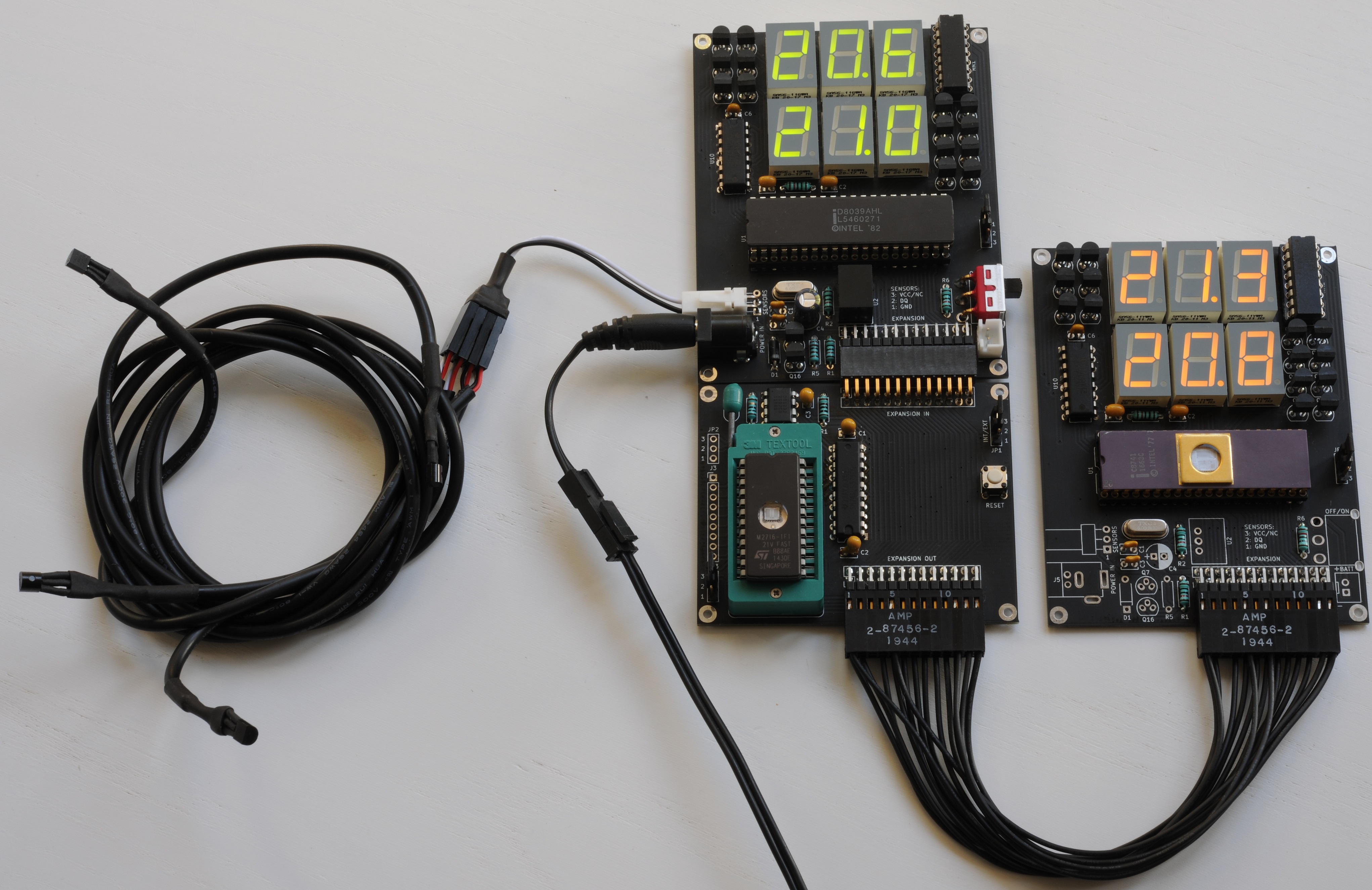
In the above demonstration the master board, fitted with an 8039 in this particular case, has four DS18B20 temperature sensors attached to it, and writes readings from sensors 3 and 4 the second board, which is simply a peripheral on the master board’s bus, with a couple of extra banks of displays on it.
Okay, so not particularly useful but does demonstrate the concept. The code for this is linked to at the end of this page. The UPI concept is repeated on modern microcontrollers, for example, on PICs it is implemented as the PSP (Parallel Slave Port).
Resources
Below I have provided everything needed to build the boards I’ve shown on this article.
Schematics
Gerbers
BOM listing
Software
- Standard 2 Sensor board listing (8035, 8039, 8×48 or 8×49)
- UPI Master listing (Requires 8039 or 8×49)
- UPI Slave listing (8741 or 8742)
Nice work, and well documented! It’s rare to see MCS-48 parts used in a recent project.
Maybe you can find something useful on my side :-). BTW, the 8748/49 can be secured using a trick I used for years. By blowing up the top FET on one of the programming pins. :-).
How these two temperature sensors are connected, are they connected in parallel? How the system will recognize we have two sensors?
https://en.m.wikipedia.org/wiki/1-Wire
Thanks
ha , the 8048 never dies…
good job.
don’t forget that like the 8031, the 8035 and 8039 often has mask code in it. the code may have failed when being mask, or was over run. I love dumping the code from these ‘romless’ chips and hand disassembling ( better than Sudoku ) to work out what it was supposed to do.
My next project will be an 8042 with latched ROM but using switch and light ( PDP8 like) console.
I had noticed that I get various garbage when I read the ROM from 8035’s. Interesting. Guess this probably wasn’t a way to get a copy of the firmware from fighter jet parts on the sneaky though.
You had better write about that 8042 project. I’ll be sure to read about it.
Not all ROMs are readable and I have found some need a specific high voltage to get the verify to output stable repeatable code. I have not had one die yet that i know of when i read as an AMP or Intel even if the High verify voltage is 2, 3 or 5 volts higher than the ‘brand’ of chip lists in the data sheet.
The link to the DevStar archive is now broken but I copied the files. Here is someone elses copy of the schematic I have been basing my fiddling on. https://aws1.discourse-cdn.com/arduino/original/4X/3/6/5/365fab88de3ad8d81328ef6638d2c13ecea9f31c.gif
I put the 8042 into reset mode to Hi-Z its interfaces , mess with the eeprom/flash then unreset the 8042.
Regarding the higher voltage to stabilize the output, I take it you are refering to the EA pin?
I’m still strugling with dumping an 80C49 (OKI manufactured, CMOS, 1983).
The bus oscillates like crazy, and seems to have a bias towards going high rather than low.
EA is pulled to well over 12.5V on the hat you constructed (thanks a bunch for doing it!)
Am also considering adding pullup or down resistors as there seems to be quite a lot of floating on the bus.
Does the code you wrote use the Arduino internal pullups?